Home Research Projects Publications Group Meetings Lab Resources Contacts

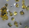
| Discovery of Chalcogenides Structures and Compositions |
Designing X-ray and Gamma Ray Detector Materials |
New Thermoelectric Materials |
 |
 |
 |
| Non-Oxidic Solids | Perovskite Solar Cells |
Nonlinear Optical Chalcogenide Materials |
 |
 |
 |
We are interested in the design, synthesis, synthetic methodology, in- depth characterization, manipulation and potential applications of new substances with novel chemical, physical, or electrical properties. These substances range from discrete molecular compounds, to solid state inorganic materials, to organic polymeric materials. We seek to obtain deeper understanding of synthesis/structure relationships and structure/function relationships.
As a graduate student interested in joining our group, you will have the opportunity to delve into cutting-edge research projects at the forefront of perovskite materials and their applications. You will work alongside experienced researchers and faculty members who are dedicated to fostering a collaborative and intellectually stimulating environment. In our group, we encourage a multidisciplinary approach, combining experimental work with computational modeling (with collaborating faculty) to gain a comprehensive understanding of a broad class of materials such as chalcogenides, perovskites and intermetallics and their behavior in devices.
We invite you to explore our website further to learn more about specific research projects, recent publications, and ongoing collaborations. Should you have any inquiries or wish to discuss potential research opportunities, please do not hesitate to reach out to us. We are excited to welcome passionate and driven graduate students who share our enthusiasm for perovskite-based technologies.
The topics of current activity include:
Discovery of Chalcogenides Structures and Compositions
Designing X-ray and Gamma Ray Detector Materials
Non-oxidic Solids with Open-Framework Structures (nano-science)
Exploratory Synthesis Presentation
NLO Presentation
Solid State Chemistry of Chalcogenides
 We are seeking talented graduate students to join our research team and delve into the captivating realm of inorganic solid-state synthesis. Unlike traditional synthetic chemists who often work with predictable molecular units, our focus lies in the exciting domain of exploratory synthesis where unpredictability reigns supreme.
In the Kanatzidis Group, we specialize in developing innovative synthetic methodologies for metal chalcogenide compounds. Our approach involves exploring the potential of molten solids as solvents for exploratory synthesis and crystal growth. Additionally, we utilize stable, pre-formed building blocks that impart specific functionality to the final structures of the solid.
Rather than approaching this chemistry solely from a high-temperature solid-state perspective, we adopt a solution chemist's outlook, drawing upon the wealth of knowledge in coordination chemistry. This unique approach allows us to gain valuable insights and make significant advancements in our field.
While advancements in techniques will undoubtedly enhance our understanding, achieving absolute synthetic predictability in any chemical synthesis is an elusive goal. However, it is precisely the unknown that both challenges and inspires us, driving our passion for exploration and pushing the boundaries of scientific discovery.
If you are an enthusiastic and driven graduate student with a passion for uncovering the mysteries of inorganic solid-state synthesis, we invite you to join our team and embark on an exhilarating research journey with us.
Recent top publications:
- ."Lithium Thiostannate Spinels: Air-Stable Cubic Semiconductors", Quintero, M. A.; Hao, S. Q.; Patel, S. V.; Bao, J. K.; Zhou, X. Q.; Hu, Y. Y.; Wolverton, C.; Kanatzidis, M. G., Chemistry of Materials 2021, 33 (6), 2080-2089, DOI: 10.1021/acs.chemmater.0c04651
- ."Vast Structural and Polymorphic Varieties of Semiconductors AMM ' Q4 (A = K, Rb, Cs, Tl; M = Ga, In; M' = Ge, Sn; Q = S, Se)", Friedrich, D.; Hao, S. Q.; Patel, S.; Wolverton, C.; Kanatzidis, M. G., Chemistry of Materials 2021, 33 (16), 6572-6583, DOI: 10.1021/acs.chemmater.1c02211.
- ."Layered and Cubic Semiconductors AGaMQ4 (A+ = K+, Rb+, Cs+, Tl+; M '4+ = Ge4+, Sn4+; Q2- = S2-, Se2-) and High Third-Harmonic Generation," Friedrich, D.; Byun, H. R.; Hao, S. Q.; Patel, S.; Wolverton, C.; Jang, J. I.; Kanatzidis, M. G., Journal of the American Chemical Society 2020, 142 (41), 17730-17742. DOI: 10.1021/jacs.0c08638
- ."The Subchalcogenides Ir2In8Q (Q = S, Se, Te): Dirac Semimetal Candidates with Re-entrant Structural Modulation," Khoury, J. F.; Rettie, A. J. E.; Robredo, I.; Krogstad, M. J.; Malliakas, C. D.; Bergara, A.; Vergniory, M. G.; Osborn, R.; Rosenkranz, S.; Chung, D. Y.; Kanatzidis, M. G., Journal of the American Chemical Society 2020, 142 (13), 6312-6323. DOI: 10.1021/jacs.0c00809
- ."In Situ Mechanistic Studies of Two Divergent Synthesis Routes Forming the Heteroanionic BiOCuSe", McClain, R.; Malliakas, C. D.; Shen, J. H.; Wolverton, C.; Kanatzidis, M. G., Journal of the American Chemical Society 2021, 143 (31), 12090-12099, DOI: 10.1021/jacs.1c03947.
- ."P2S5 Reactive Flux Method for the Rapid Synthesis of Mono- and Bimetallic 2D Thiophosphates M2-xM ' xP2S6", Chica, D. G.; Iyer, A. K.; Cheng, M.; Ryan, K. M.; Krantz, P.; Laing, C.; dos Reis, R.; Chandrasekhar, V.; Dravid, V. P.; Kanatzidis, M. G., Inorganic Chemistry 2021, 60 (6), 3502-3513, DOI: 10.1021/acs.inorgchem.0c03577.
- ."Panoramic Synthesis as an Effective Materials Discovery Tool: The System Cs/Sn/P/Se as a Test Case", Haynes, A. S.; Stoumpos, C. C.; Chen, H. J.; Chica, D.; Kanatzidis, M. G., Journal of the American Chemical Society 2017, 139 (31), 10814-10821. DOI: 10.1021/jacs.7b05423
- ."Direct thermal neutron detection by the 2D semiconductor (LiInP2Se6)-Li-6," Chica, D. G.; He, Y. H.; McCall, K. M.; Chung, D. Y.; Pak, R. O.; Trimarchi, G.; Liu, Z. F.; De Lurgio, P. M.; Wessels, B. W.; Kanatzidis, M. G., Nature 2020, 577 (7790), 346-349. DOI: 10.1038/s41586-019-1886-8
- ."Sn4-? B12Se12 [Qx], Q = Se, Te, a B12 Cluster Tunnel Framework Hosting Neutral Chalcogen Chains", Chica, D. G.; Spanopoulos, I.; Hao, S. Q.; Wolverton, C.; Kanatzidis, M. G., Chemistry of Materials 2021, 33 (5), 1723-1730, DOI: 10.1021/acs.chemmater.0c04503.
- ."Photoluminescent Re6Q8I2 (Q = S, Se) Semiconducting Cluster Compounds", Laing, C. C.; Shen, J. H.; Chica, D. G.; Cuthriell, S. A.; Schaller, R. D.; Wolverton, C.; Kanatzidis, M. G., Chemistry of Materials 2021, 33 (14), 5780-5789, DOI: 10.1021/acs.chemmater.1c01696.
Science and Applications of Halide Perovskites
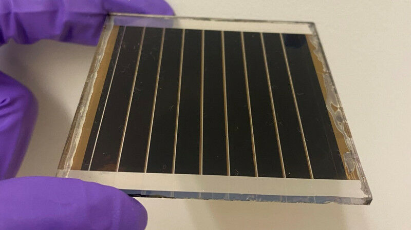 We are engaged in an exciting range of projects centered around organic-inorganic halide perovskite materials for solar cells and optoelectronics applications. Our work encompasses diverse areas, including design, synthesis, fundamental studies, and device fabrication, all aimed at advancing the field of perovskite-based chemistry and technologies.
At the core of our research, we focus on exploring novel perovskite materials with varying dimensionalities. Through meticulous design and synthesis efforts, we strive to achieve phase-pure compositions, ensuring the highest material quality. Our team places great emphasis on precise crystallographic structure determination, employing advanced techniques to gain a thorough understanding of the crystal lattice and its arrangement. Additionally, we conduct comprehensive property measurements, allowing us to analyze the behavior of these perovskite materials in different conditions. To complement our experimental investigations, we employ electronic structure calculations to provide insights into the underlying physical mechanisms and properties.
In line with our research interests, we are actively involved in the development and fabrication of various devices for solar energy conversion and radiation detection. Our aim is to harness the unique properties of perovskite materials to enhance the efficiency and performance of these devices. Whether it's solar cells for converting sunlight into electricity or radiation detectors for precise measurement and imaging, we explore innovative device architectures and fabrication techniques to maximize their potential.
Back to Top
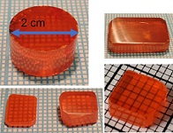
Gamma Ray Detector Materials
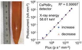 In this project we focus on groundbreaking advancements in X-ray and γ-ray radiation detection using new materials. Discovering highly sensitive hard radiation detectors that operate at room temperature is crucial for a wide range of applications.
One of the fascinating materials we're investigating is the perovskite semiconductor CsPbBr3, which exhibits exceptional spectral resolution for γ-rays at room temperature. CsPbBr3 boasts several advantageous properties: it is air-stable, non-hygroscopic, and possesses a high effective atomic number (Z-eff) of 65.9.
Our research efforts have led to exciting progress in the field of CsPbBr3 crystals. We provide an overview of the research conducted on bulk CsPbBr3 crystals and the development of highly pure crystals through effective procedures. By utilizing the Bridgman method, we have successfully grown single crystals with enhanced quality and larger sizes, significantly reducing impurities to an impressive less than 9 ppm of the combined amount of 69 different impurity elements, as measured by Glow Discharge Mass Spectrometry.
CsPbBr3 perovskite's defect tolerance allows us to achieve remarkable transport properties for both carriers, with high carrier mobility. The exceptional carrier mobility exceeds 5x10⁻³ cm2/V for holes and surpasses 10-3 cm2/V for electrons.
In our research, we've demonstrated the outstanding energy-resolving capability of CsPbBr3 detectors under both X and γ-rays. Notably, we achieved a remarkable energy resolution of 3.9% (FWHM) for 122 keV 57Co γ-ray with good temporal stability. Furthermore, our CsPbBr3 detector-grade single crystal has shown a hole lifetime well over 25 µs.
We've also developed 2x2 pixelated devices that offer impressive energy resolution, resolving 137Cs 662-keV γ-rays with just 1.4% energy resolution. Additionally, our detectors are capable of accurately detecting X- and γ-rays with energies ranging from tens of keV to over 1 MeV in unipolar hole-only sensing modes.
If you are passionate about cutting-edge research in radiation detection and want to be part of a dynamic team pushing the boundaries of material science, join our research group today and embark on an exciting journey of scientific discovery!
Back to Top
New Thermoelectric Materials
Presentation 1
Presentation 2
Presentation 3 (added 11/09)
Presentation 4 (added 10/2011)
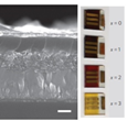
The challenge to create high efficiency thermoelectric (TE) materials lies in achieving simultaneously high electronic conductivity, high thermopower and low thermal conductivity in the same material. These properties define the thermoelectric figure of merit ZT = (S2σ /κ )T; where S is the thermopower, σ the electronic conductivity, κ the thermal conductivity, and T the temperature. The first three quantities are determined by the details of the electronic structure and scattering of charge carriers (electrons or holes) and thus are not independently controllable parameters. The thermal conductivity has a contribution from lattice vibrations, κlat which is called the lattice thermal conductivity. Thus κ = κe + κlat , where κe is the carrier thermal conductivity.
In the Kanatzidis group, we aim to synthesize new bulk materials with high ZTs greater than the historic threshold of ZT=1 with two general approaches. By adding nanostructure to the matrix of the pristine material, the lattice thermal conductivity component in the denominator of ZT can be significantly reduced , resulting in dramatic increases in ZT. A different, less understood method for increasing ZT is to increase the power factor S2σ by increasing the thermopower of material without depressing the electronic conductivity. The relationship between thermopower and electrical conductivity is quite complex, but it may be possible to alter one and not the other with band structure engineering.
Our group focuses on the lead chalcogenides, PbTe, PbSe, and PbS and Bi2Te3, and recently SnTe.
Bi2Te3 Materials
Bi2Te3 is one of the major constituents in the best thermoelectric materials for use near room temperature. It is the most promising compound for the application of thermoelectric materials for refrigeration. Solid solution alloying with Sb2Te3 and Sb2Se3 can improve the thermoelectric figure of merit. Triggered by this, our group focuses on the p- and the n- type Bi2Te3 based semiconductors aiming the optimization of their thermoelectric properties.
PbTe-Based Materials
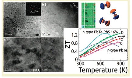
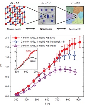 PbTe thermoelectric materials are the champions of high ZT. Our group has synthesized several materials with ZTs above 1.7, and recently as high as 2.2 By doping PbTe with PbS and Na, we can control nanostructure formations (to reduce κlat) while concurrently modifying the electronic structure to significantly enhance the thermoelectric powerfactor. In the PbTe-PbS 12%-Na 2% system, Na produces shape controlled cubic PbS nanostructures which help reduce κlat, while altering the solubility of PbS within the PbTe matrix beneficially modifies the DOS to allow for enhancement of the power factor to give a ZT of 1.8 at 800K (Girard, et. al, J. Am. Chem. Soc., 2011, 133, 15588).
Another novel high ZT system, PbTe-PbSr 2%-Na 2% utilizes endotaxially arranged SrTe nanocrystals incorporated in the PbTe matrix to reduce κlatwithout having a detrimental effect on carrier mobility unlike previous nanostructured thermoelectrics. The endotaxial SrTe nanoprecipitates inhibit the heat flow in the system, but the crystallographic alignment of the SrTe and PbTe does not affect the hole mobility, allowing a large power factor to be achieved concurrently with a very low thermal conductivity. This decoupling of phonon and electron transport allows the system to reach ZT=2.2 at 900K (Biswas, et. al, Nature, 2012, 489,414.)
PbSe Based materials
The binary narrow band gap semiconductor PbSe combines several attractive features for potential thermoelectric applications such as a favorable electronic valence band structure that is comprised of two sub-bands with very different effective masses in similarity to that of PbTe, lower cost, and higher operation temperatures. Although high ZTs have been reported for several n-type PbSe compositions (ZT = ~0.9 at 900 K : Androulakis, et. al, Phys. Rev. B., 2011, 83, 195209 and ZT = ~1.3 at 900 K : Androulakis, et. al, J. Am. Chem. Soc., 2011, 133, 28), theoretical calculations suggest that heavily doped p-type PbSe can potentially show a ZT ~2 at 1000 K (Parker, et. al, Phys. Rev. B., 2010, 82,035204).
PbS Based materials
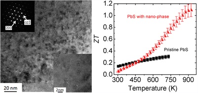
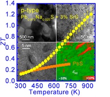
PbTe based thermoelectric materials show high performance at room and middle temperature range (600-850K), however, they contain significant amount of Te, which is a scarce element in the crust of the earth. Hence the Te price is likely to rise sharply if Te based thermoelectric materials reach mass markets. A broad search for more inexpensive alternatives is therefore warranted. S is very earth abundant compared to Te and Se, and the Pb is very strongly bound to S, making it environmentally safe. Recently, we proposed PbS as an ideal candidate for widespread application of environmentally stable and affordable thermoelectric material system because high performance in both n-type (ZT~1.1 at 923 K) and p-type (ZT~1.2 at 923 K) can be achieved. We showed that the lattice thermal conductivity can be reduced to very low levels through nanostructuring with metal sulfides such as Bi;2S;3 and Sb;2S;3 in n-type and SrS and CaS in p-type (Zhao, et. al. J. Am. Chem. Soc., 2011, 133, 20476-20487 and Zhao, et. al. J. Am. Chem. Soc., 2012, 134, 7902-7912.)\
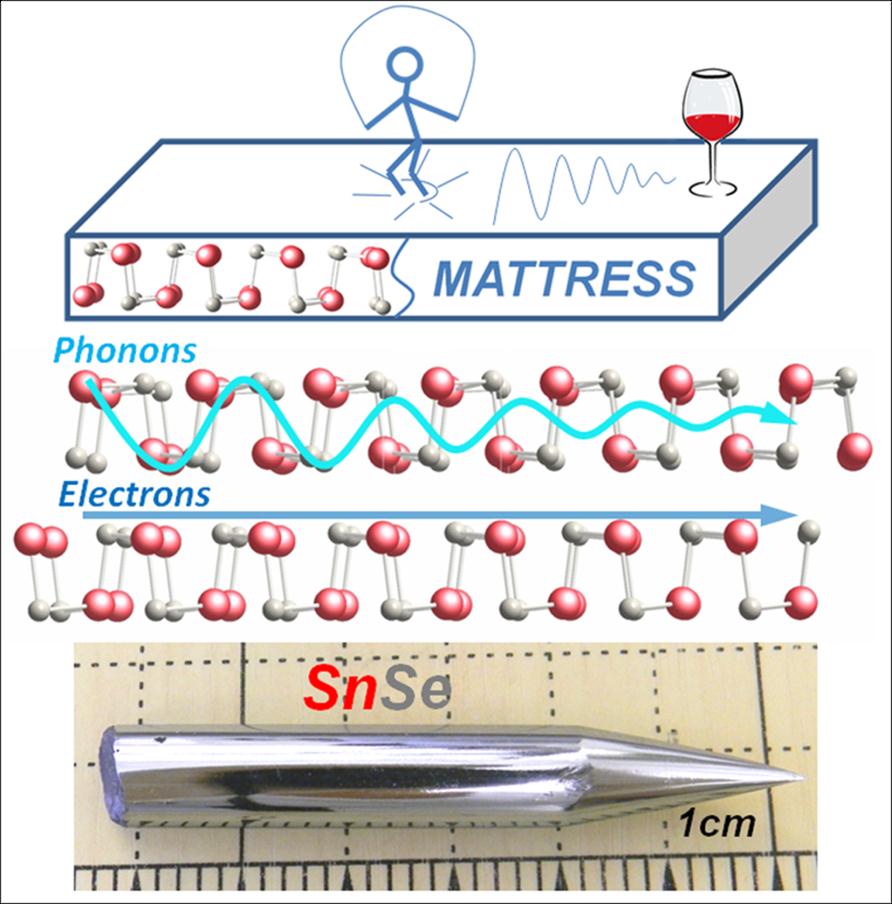
SnSe materials
SnSe is the worlds least thermally conductive crystalline material. Heat cannot travel well through this material because of its very soft, accordion-like layered structure which does not transmit vibrations well. It reminds us of the TV commercial for posture-pedic mattress where one can jump up and down on one side of the mattress and a few feet away a glass of wine does not feel the vibrations. By analogy SnSe can get hot on one side and the other side remains cool. The cool side does not feel the vibrations (also known as phonons). In SnSe this means that all heat must go to the other side of the crystal riding on the electronic carriers, not lattice vibrations. Thus, the hot carriers can generate useful electricity during their transport. That is enabled by the high thermoelectric power of SnSe. The poor ability to carry heat through its lattice enables the resulting record high thermoelectric conversion efficiency.
This outstanding property can be exploited in solid state electronic devices which can directly convert heat to electricity. Places where there is high heat and high temperature such as exhaust gas from coal and gas-fired power plans, automobile exhaust, high temperature processing (glass and brick industries, etc).
Journal Reference:
Li-Dong Zhao, Shih-Han Lo, Yongsheng Zhang, Hui Sun, Gangjian Tan, Ctirad Uher, C. Wolverton, Vinayak P. Dravid, Mercouri G. Kanatzidis. Ultralow thermal conductivity and high thermoelectric figure of merit in SnSe crystals. Nature, 2014; 508 (7496): 373 DOI: 10.1038/nature13184
Interest in TE materials is not new but the need for new materials is increasing and the next decade will be critical in the development of this field. Taking into account the difficulty if identifying the "right" compound and optimizing to ZT > 1, long term sustainable planning is necessary and close collaboration between chemists, physicists and engineers is key to success. Such collaborative approaches have been the paradigm in which the present effort is base
Collaboration with Tellurex
Inc.
Back to Top
Non-oxidic Solids with Open-Framework Structures
(nano-science)
Layered Metal Sulfides
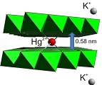
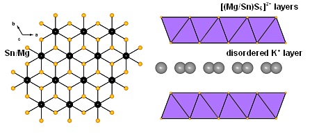
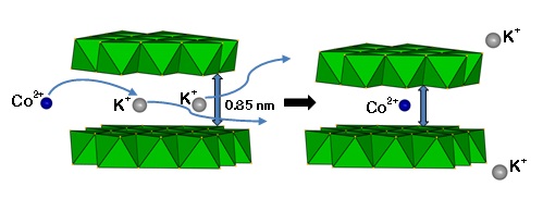
Layered metal sulfide materials of the general formula A2xMxSn3-xS6 (x=0.5-0.95; A = Li+, Na+, K+, Rb+; M = Mg2+, Mn2+, Zn2+, Fe2+) made of inexpensive, non-toxic elements that can be easily prepared on a large scale with high purity are highly desireable. Using solid-state or hydrothermal synthesis techniques these materials are extremely stable in an air atmosphere and water. Layered metal sulfide materials exhibit facile and highly selective ion-exchange properties for cations of great environmental concern such as Cs+ and Sr2+; the radioactive isotopes of which are the major contaminants in the fission product of nuclear wastes. They are also extremely capable to clean the water from soft heavy metal ions (e.g. Hg2+, Pb2+, Cd2+, Ag+), which constitute a serious health threat for humans and other species.
Back to Top
New Nonlinear Optical Chalcogenide Materials
NLO Presentation
The objective of this project is to generate high-quality single crystals of new
chalcogenide materials that exhibit some of the most active nonlinear optical (NLO)
properties discovered to date. The project involves detailed optical investigations,
comprehensive measurements of NLO constants in various crystal directions, and laser
stability assessments. By employing advanced solid-state synthesis techniques
combined with purification strategies and crystal growth investigations, the project aims
to understand the crystallization properties of these materials. Once the quality and
single-crystal nature of the samples are confirmed, they will be studied in collaboration
with Prof. V. Gopalan at Penn State University. This will include extensive laser NLO
measurements, determining the complete second-order tensor, examining symmetry
and symmetry-breaking effects, measuring the laser damage threshold (LDT), and
analyzing nonlinear multiphoton absorption and refraction. Specific objectives include
synthesizing highly pure chalcogenide materials with strong NLO responses, growing
sizable single crystals, measuring all fundamental NLO properties, and assessing the
LDT of the most promising materials.
The project focuses on investigating several classes of low-dimensional chalcogenide
materials, including alkali-metal chalcoarsenate systems (A-As-Q; A=Li, Na, K; Q=S,
Se), chalcophosphates (A-P-Se), and chalcogermanate systems (A-Ge-Q). The key
characteristics sought in these materials include ease of synthesis with scalable
precursors, congruent melting behavior at reasonable temperatures (<900°C) for large-
volume crystal growth using the Bridgman method, high transmission at pump
wavelengths around 1µm, absence of two-photon absorption at the pump wavelength,
high transmission in the mid-IR range up to 15µm, high nonlinearity, high optical
damage threshold, engineerability for compositional variation, low hygroscopicity, high
transmission in the FIR range (60µm - 300µm), a wide bandgap (>1.5 eV), and
absence of phase transitions that could hinder crystal growth from the melt. When a
material lacks some desirable properties, alternative crystal growth methods such as
flux growth, hydrothermal synthesis, and chemical vapor transport will be pursued.
Single crystals will be grown using three methods: cooling of melts, inert salt fluxes, and
chemical vapor transport. The efficacy of these methods will be assessed, and the
highest optical quality crystals will be sent to the Gopalan Lab for comprehensive optical
studies, including second harmonic generation (SHG), difference frequency generation
(DFG), linear optical properties, laser damage threshold, and nonlinear absorption and
refraction characterization.
This is a collaborative research project led by Mercouri Kanatzidis and James Rondinelli
at Northwestern University, with Venkatraman Gopalan from Penn State University. We
investigate specific classes of low-dimensional chalcogenide materials, focusing on their
synthesis, growability, and fundamental NLO properties. Key characteristics sought
include high nonlinearity, broad IR transparency, high laser damage threshold, and ease
of synthesis with scalability. Techniques like the Bridgman method, flux growth, and
chemical vapor transport are employed to grow single crystals, which are then
characterized for their optical properties at Penn State University. The project also aims
to address challenges such as phase transitions and incongruent melting behavior
through chemical substitutions and alternative growth methods. The successful
development of these materials could significantly impact IR technologies relevant to
the Department of Defense, including IR laser systems, remote sensing, and
countermeasures.

Back to Top
For examples of work in each of these areas see List of Publications.