Research
Our group focuses on “making precious metals more precious” by controlling the size and shape of noble metals at the nanoscale.
Our strategies include the development of new nanofabrication tools to create three-dimensional architectures with structural function that can span three-orders of magnitude simultaneously. We are also pursuing simple and scalable approaches to synthesize anisotropic particles. To understand the details of how light interacts with these structures, we use modeling to calculate the optical properties of single particles as well as the collective effects of assemblies of nanoparticles. Applications of these unique materials include nanomedicine, photovoltaics, sensing, and imaging.
Learn More
- Visit News Archive
- Browse our Publications
- Inquiries? Contact Us
Nanomedicine and Bioimaging
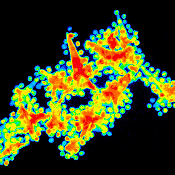
Direct visualization of interactions between drug-loaded nanoparticles and the cancer cell nucleus is crucial for understanding how to improve the efficacy of therapeutics. We have recently designed nanoconstructs composed of nucleolin-specific aptamers and gold nanostars that not only can target cancer cells but can be actively transported to the nucleus and then induce major changes in nuclear phenotype. We are developing these nanoconstructs as a new type of drug delivery system since their “cargo” can be released using ultra-fast, laser light. Also, we are interested in probing how nanoparticles behave intracellularly and are focusing on uptake and transport mechanisms.
Nanophotonics and Nano-optics
Coherent light sources at the nanoscale are important for investigating phenomena in small dimensions and for realizing optical devices with sizes that can beat the diffraction limit of light. Plasmonic lasers can have sub-wavelength sizes because they exploit surface plasmons which have strongly confined electromagnetic fields. We are interested in designing laser devices based on coupled plasmonic nanoparticles and that are the size of a virus particle. In addition, we are designing new types of metal lenses based on a metamaterial concept with properties not possible in conventional lenses.
Materials and Nanofabrication
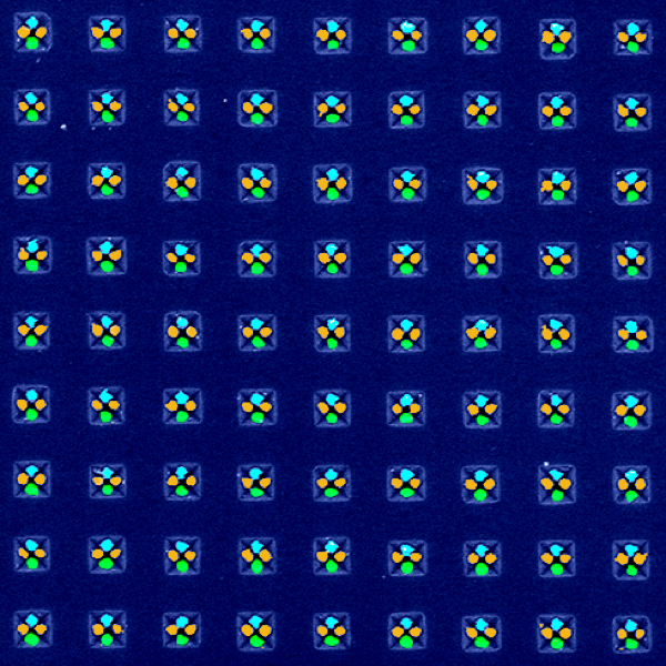
One important challenge in nanoscience is the development of innovative tools that can manipulate nanoscale building blocks into hierarchical structures over large areas. This control requires a detailed understanding over several length scales in order to achieve (1) precise nanoscale (1-100 nm) manipulation and (2) assembly into mesoscale (100-1000 nm) structures. We are working on many different materials systems, including patterning liquid metals to achieve switchable optical properties, creating nanowrinkles in polymer films based on chemical treatment of the surface, and inventing new lithographies such as moiré nanolithography that can result in high-order rotational symmetry lattices.

Meet Our Sponsors